The Introduction
For this post I will walk you through a project with a Field Programmable Gate Array (FPGA), which was interfaced with a hand constructed clock circuit (an astable multivibrator).
I. The FPGA Overview
A Field Programmable Gate Array (FPGA) is a tool which can be used for high performance computing applications. FPGA’s work directly in the hardware layer (even machine language works on top of hardware). An FPGA is a prototyping tool where the chip circuitry is programmed. When you program an FPGA, you are rearranging circuits in your processor/controller.
II. The Basics
A. Circuit Basics
For this project we need to build a circuit on a breadboard. Here are the fundamentals I used in order to get my circuit working.
Transistors are a special type of circuit component. The way we will use them is as a switch. When the transistor is turned on, it acts like there is just a wire connecting the input and output (a closed circuit). When the transistor is off, it’s as if the input and output aren’t connected at all (an open circuit). The transistor is ‘on’ when current is supplied to its third wire (called the base) and off otherwise.
RC circuits are a way to add timing to a circuit. Capacitors store charge up until a certain point, and the time it takes to charge up (time constant) is very calculable. The time constant for a given RC circuit is the value of the resistor in Ohms multiplied by the value of the capacitor in Farads. The Ohms and Farads cancel out to seconds. The resultant value is how long it takes the capacitor in your RC circuit to reach full charge. You can design the rest of your circuit to react when this charging completes.
Ohm’s Law: V = IR. V is voltage, I is current, and R is resistance. This equation will primarily help with making sure voltage values are in line for our application. In order for our external circuit to interface with the FPGA, the output from this circuit needs to be around 3.3V (as in 3.3V or less, or else we could damage our FPGA). The current for our circuit will be determined by our battery and our resistor values will be determined by the RC circuit. What ends up happening is that we add extra resistors between the circuit’s output and the FPGA, as opposed to trying to get the circuit to naturally output the correct voltage.
In order to make an astable multivibrator (square wave generator/clock circuit) we will essentially create two RC circuits, each of which connects to a transistor which turns the other on/off. As one charges, the other is in a discharge state, then when charging is complete the other circuit enters a charge state and the original circuit enters a discharge state, and on and on. If you bleed off a certain point in the circuit as output, you have a signal that predictably has voltage and then no voltage (a clock signal, or a square wave), which is what we want.
B. Mojo v3 Basics
The Mojo v3 is the development board that I have. If you do not have an FPGA and are looking to experiment with one, this is a disclaimer. These devices can be expensive and being able to download the software to develop on them is not straightforward (for the Mojo v3, there is no open source alternative, and hoops had to be jumped through to gain licensure with Xilinx to be able to build projects with the provided IDE). When you decide on a development board, I recommend following all steps to be able to develop for the chip, up until actually loading it onto the FPGA, before you buy.
Programming the Mojo v3 (and I assume any FPGA) is like programming a microcontroller or doing any very low level work. The variable types (if you can call them variables) are very different from the logical abstractions of integer and double, etc. Instead you handle bits and groups of bits in the form of what lexically look like arrays. And you set values to 1 or 0, which represent high and low voltage. You can abstract these as numbers, but you can also manipulate them as the grouped voltages that they are.
III. The Project
A. External Circuit
As hinted at, we will interface a clock signal (as supplied by our astable multivibrator) with our FPGA (Mojo v3 development board, which uses the Spartan-6 FPGA chip).
Astable Multivibrator Circuit Schematic:
From the Wikipedia Page about Multivibrators (https://en.wikipedia.org/wiki/Multivibrator)
My Diagram for How Electricity Flows through the Circuit:

Astable multivibrator circuit schematic showing how current flows when the left capacitor is discharging and the right capacitor is charging (one of two opposite states)
The zig-zags are resistors, the parallel lines are capacitors, the >| with circles are LED’s and the >| near the bottom (look like the LED’s but have an arrow in the circle as well) are transistors. There are three different ‘wavy lines’ which represent the flow of current for each major part. The point is that while one LED is on, the other is off, and they switch states indefatigably.
Actual Circuit:
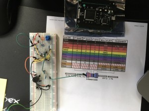
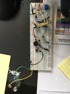
I added some modifications to my circuit, one of which is for debugging purposes and the other has actual practical value. There is a black cylinder on my breadboard, that is a speaker that replaced one of the LED’s; I can hear the clock tic. But the really useful bit is the potentiometer (blue thing at the top with a knob). That allows me to haptically (physically with my hand) change the timing of the clock, it allows me to change the time between tics by turning that knob. Additionally, that green wire sticking out the right side is the output for the FPGA; it bleeds voltage from where the LED is. (Not to mention I added a button which turns the circuit on when held down — also the battery I’m using is a 9V because that is what I had.)
Now, taking a schematic and turning it into something you can use takes practice. Get out your multimeter and play around before actually plugging anything into your FPGA. This is a nice starter kit (this is what I have) for getting into building circuits.
Remember that this is how computing got started; before computer science, there was electrical engineering with transistors (which weren’t always made out of doped silicon and nanometers in size).
B. FPGA Code
Now that we have our circuit, let’s talk about programming an FPGA.
// MODIFIED FILE: blinker.luc

module blinker (
    input clk,    // clock
    input rst,    // reset
    output blink,  // output to LED
    input pinIn // input for external astable multivibrator circuit
  ) {

  .clk(clk), .rst(rst) {
  }

  always {
    blink = bx;
    case (pinIn) {
    0:
        blink = b0;
    1:
        blink = b1;
    }
  }
}
In the above figure, note that ‘pinIn’ is attached to a case/switch statement, as opposed to setting the value of ‘blinker’ to the ‘pinIn’ state. This will be used for later projects to elicit behavior other than setting a light on/off. The pinIn voltage is the voltage of the output from our circuit.
// MODIFIED FILE: mojo_top.luc
module mojo_top (
    input clk,              // 50MHz clock
    input rst_n,            // reset button (active low)
    output led [8],         // 8 user controllable LEDs
    input cclk,             // configuration clock, AVR ready when high
    output spi_miso,        // AVR SPI MISO
    input spi_ss,           // AVR SPI Slave Select
    input spi_mosi,         // AVR SPI MOSI
    input spi_sck,          // AVR SPI Clock
    output spi_channel [4], // AVR general purpose pins (used by default to select ADC channel)
    input avr_tx,           // AVR TX (FPGA RX)
    output avr_rx,          // AVR RX (FPGA TX)
    input avr_rx_busy       // AVR RX buffer full
  ) {

  sig rst;                  // reset signal
  sig pn; // pinIn signal

  .clk(clk) {
    // The reset conditioner is used to synchronize the reset signal to the FPGA
    // clock. This ensures the entire FPGA comes out of reset at the same time.
    reset_conditioner reset_cond;

    .rst(rst), .pinIn(pn) {
     blinker myBlinker;
    }
  }

  always {
    reset_cond.in = ~rst_n;    // input raw inverted reset signal
    rst = reset_cond.out;      // conditioned reset

    led = 8x{myBlinker.blink}; // blink LEDs
    spi_miso = bz;             // not using SPI
    spi_channel = bzzzz;       // not using flags
    avr_rx = bz;               // not using serial port
  }
}
// CONSTRAINT FILE: pinIn.ucf
NET "pinIn" LOC = P1 | IOSTANDARD = LVTTL;
Most of this is boilerplate that comes with the Mojo v3 IDE. The important part is the pinIn.ucf. It is in that file where I tell the FPGA to look at PIN 1 for an input (which could be anything, but in this case it will be our circuit).
This amazing resource is Embedded Micro. They made the Mojo v3. That link takes you to the landing page for all of their tutorials for making all sorts of programs.
For what I have here (and specifically for the Mojo v3), all you need to do is open a new project based upon the ‘Blinker Demo’ and make the modifications above, such as adding the Component pinIn.ucf and somewhat altering blinker.luc and altering mojo_top.luc.
The Conclusion
After plugging the green output wire into the PIN 1 hole on the FPGA development board, the LED strip on the Mojo v3 will blink in unison with the clock signal from your circuit, way cool! But this is just the beginning. Consider this the ‘Hello World’ of interfacing a circuit with an FPGA. FPGA’s can do much more than pipe an input wire to an LED. And FPGA’s are meant for high performance computing. (FPGA’s can make very complex decisions very quickly, for very specific applications).
Think about this as if a user interface has been created for your high performance hardware solution in the form of an external circuit. Consider interfacing a circuit with your FPGA to be implementing a UI framework where using the API involves constructing something physical with resistors and capacitors; that’s how you have to do it when developing at this low of a level. Happy hacking!


